The PCB materials industry has spent significant amounts of time developing materials that provide lowest possible signal loss. For high speed and high frequency designs, losses will limit signal propagation distance and distort signals, and it will create an impedance deviation that can be seen in TDR measurements. As we design any printed circuit board and develop circuits that operate at higher frequencies, it may be tempting to opt for the smoothest possible copper in all designs you create.
While it is true that copper roughness creates additional impedance deviation and losses, how smooth does your copper foil really need to be? Are there some simple methods you can use to overcome losses without selecting ultra-smooth copper for every design? We’ll look at these points in this article, as well as what you can look for if you start shopping for PCB stackup materials.
Types of PCB Copper Foil
Normally when we talk about copper on PCB materials, we don’t talk about the specific type of copper, we only talk about its roughness. Different copper deposition methods produce films with different roughness values, which can be clearly distinguished in a scanning electron microscope (SEM) image. If you’re going to be operating at high frequencies (normally 5 GHz WiFi or above) or at high speeds, then pay attention to the copper type specified in your material datasheet.
Also, make sure to understand the meaning of Dk values in a datasheet. Watch this podcast discussion with John Coonrod from Rogers to learn more about Dk specifications. With that in mind, let’s look at some of the different types of PCB copper foil.
Electrodeposited
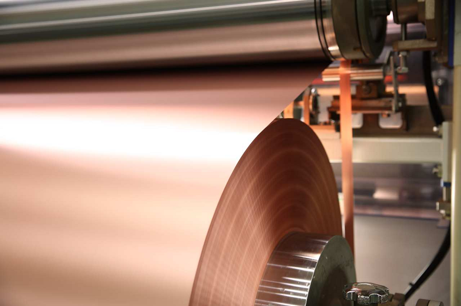
In this process, a drum is spun through an electrolytic solution, and an electrodeposition reaction is used to “grow” the copper foil onto the drum. As the drum rotates, the resulting copper film is slowly wrapped onto a roller, giving a continuous sheet of copper that can later be rolled onto a laminate. The drum side of the copper will essentially match the roughness of the drum, while the exposed side will be much rougher.
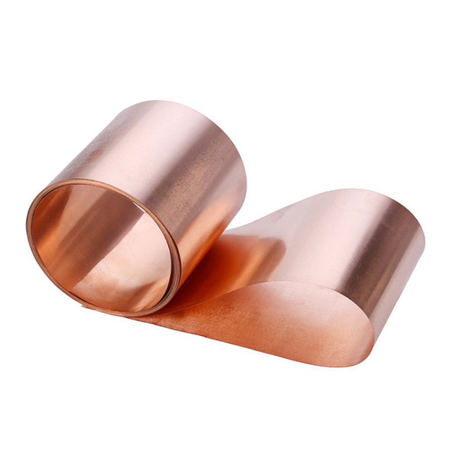
Electrodeposited PCB copper foil
Electrodeposited copper production.
In order to be used in a standard PCB fabrication process, the rough side of the copper will first be bonded to a glass-resin dielectric. The remaining exposed copper (drum side) will need to be intentionally roughened chemically (e.g., with plasma etching) before it can be used in the standard copper clad lamination process. This will ensure it can be bonded to the next layer in the PCB stackup.
Surface-Treated Electrodeposited Copper
I don’t know the best term that encompasses all the different types of surface treated copper foils, thus the above heading. These copper materials are best known as reverse treated foils, although two other variations are available (see below).
Reverse treated foils use a surface treatment that is applied to the smooth side (drum side) of an electrodeposited copper sheet. A treatment layer is just a thin coating that intentionally roughens the copper, so it will have greater adhesion to a dielectric material. These treatments also act as an oxidation barrier that prevents corrosion. When this copper is used to create laminate panels, the treated side is bonded to the dielectric, and the leftover rough side remains exposed. The exposed side will not need any additional roughening before etching; it will already have enough strength to bond to the next layer in the PCB stackup.
Three variations on reverse treated copper foil include:
High temperature elongation (HTE) copper foil: This is an electrodeposited copper foil that complies with IPC-4562 Grade 3 specifications. The exposed face is also treated with an oxidation barrier to prevent corrosion during storage.
Double-treated foil: In this copper foil, the treatment is applied to both sides of the film. This material is sometimes called drum-side treated foil.
Resistive copper: This is not normally classified as a surface-treated copper. This copper foil uses a metallic coating over the matte side of the copper, which is then roughened to the desired level.
Surface treatment application in these copper materials is straightforward: the foil is rolled through additional electrolyte baths that apply a secondary copper plating, followed by a barrier seed layer, and finally an anti-tarnish film layer.
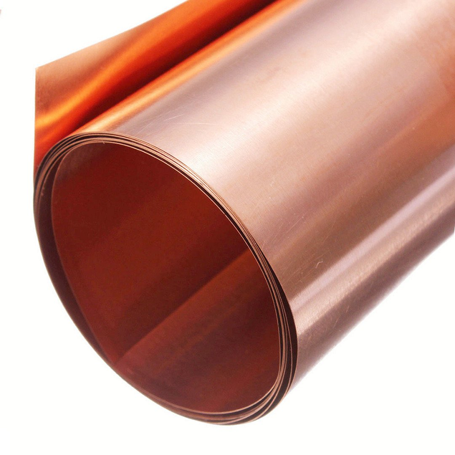
PCB copper foil
Surface treatment processes for copper foils. [Source: Pytel, Steven G., et al. "Analysis of copper treatments and the effects on signal propagation." In 2008 58th Electronic Components and Technology Conference, pp. 1144-1149. IEEE, 2008.]
With these processes, you have a material that can be easily used in the standard board fabrication process with minimal additional processing.
Rolled-Annealed Copper
Rolled-annealed copper foils will pass a roll of copper foil through a pair of rollers, which will cold-roll the copper sheet to the desired thickness. The roughness of the resulting foil sheet will vary depending on the rolling parameters (speed, pressure, etc.).
The resulting sheet can be very smooth, and striations are visible on the surface of the rolled-annealed copper sheet. The images below show a comparison between an electrodeposited copper foil and a rolled-annealed foil.
PCB copper foil comparison
Comparison of electrodeposited vs. rolled-annealed foils.
Low-Profile Copper
This is not necessarily a type of copper foil you would fabricate with an alternative process. Low-profile copper is electrodeposited copper that is treated and modified with a micro-roughening process to provide very low average roughness with sufficient roughening for adhesion to the substrate. The processes for manufacturing these copper foils is normally proprietary. These foils are often categorized as ultra-low profile (ULP), very low profile (VLP), and simply low-profile (LP, approximately 1 micron average roughness).
Related articles:
Why is Copper Foil used in PCB Manufacturing?
Copper Foil Used in Printed Circuit Board
Post time: Jun-16-2022