Copper foil has low rate of surface oxygen and can be attached with a variety of different substrates, such as metal, insulating materials. And copper foil is mainly applied in electromagnetic shielding and antistatic. To place the conductive copper foil on the substrate surface and combined with the metal substrate, it will provide excellent continuity and electromagnetic shielding. It can be divided into: self-adhesive copper foil, single side copper foil, double side copper foil and the like.
In this passage, if you are going to learn more about copper foil in the PCB manufacturing process, please check and read the content below in this passage for more professional knowledge.
What are the features of copper foil in the PCB manufacturing?
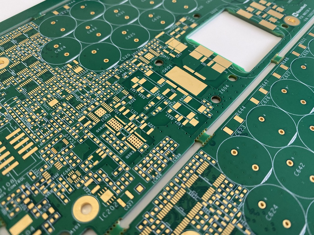
PCB copper foil is the initial copper thickness applied on outer and inner layers of a multilayer PCB board. Copper weight is defined as the weight (in ounces) of copper present in one square foot of area. This parameter indicates the overall thickness of copper on the layer. MADPCB utilizes the following copper weights for PCB fabrication (pre-plate). Weights measured in oz/ft2. The appropriate copper weight can be selected to fit the design requirement.
· In PCB manufacturing, the copper foils are in rolls, which are electronic grade with purity of 99.7%, and thickness of 1/3oz/ft2 (12μm or 0.47mil) – 2oz/ft2 (70μm or 2.8mil).
· Copper foil has lower rate of surface oxygen and can be pre-attached by laminate manufacturers to various base materials, such as metal core, polyimide, FR-4, PTFE and ceramic, to produce copper clad laminates.
· It also can be introduced in a multilayer board as copper foil itself before pressing.
· In conventional PCB manufacturing, the final copper thickness on inner layers remains of the initial copper foil; On outer layers we plate extra 18-30μm copper on the tracks during the panel plating process.
· The copper for the outer layers of multilayer boards is in the form of copper foil and pressed together with the prepregs or cores. For use with microvias in HDI PCB, the copper foil is directly on RCC (resin coated copper).
Why copper foil is needed in the PCB manufacturing?
Electronic grade copper foil (purity of more than 99.7%, thickness 5um-105um) is one of the basic materials of the electronics industry The rapid development of electronic information industry, the use of electronic grade copper foil is growing, the products are widely used in industrial calculators, Communications equipment, QA equipment, lithium-ion batteries, civilian television sets, video recorders, CD players, copiers, telephone, air conditioning, automotive electronics, game consoles.
Industrial copper foil can be divided into two categories: rolled copper foil (RA copper foil) and point copper foil (ED copper foil), in which the calendaring copper foil has good ductility and other characteristics, is the early soft plate process used Copper foil, while the electrolytic copper foil is a lower cost of manufacturing copper foil. As the rolling copper foil is an important raw material of the soft board, so the characteristics of calendaring copper foil and price changes on the soft board industry have a certain impact.
What are the basic design rules of copper foil in PCB?
Do you know that printed circuit boards are very common in the group of electronics? I am pretty much sure one is present in the electronic device you are using right now. However, using these electronic devices without understanding their technology and the designing method is also a common practice. People are using electronic devices every single hour but they don’t know how they work. So here are some main parts of PCB that are mentioned to have a quick understanding of how printed circuit boards work.
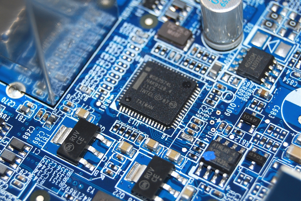
· The printed circuit board is simple plastic boards with the addition of glass. The copper foil is used for tracing the pathways and it allows the flow of charges and signals within the device. Copper traces are the way to provide power to different components of the electrical device. Instead of wires, copper traces guide the flow of charges in PCBs.
· PCBs can be one layer and two layers also. One layered PCB is the simple ones. They have copper foiling on one side and the other side is the room for the other components. While on the double-layered PCB, both sides are reserved for copper foiling. Double layered are the complex PCBs having complicated traces for the flow of charges. No copper foils can cross each other. These PCBs are required for heavy electronic devices.
· There are also two layers of solders and silkscreen on copper PCB. A solder mask is used to distinguish the color of the PCB. There are many colors of PCBs available such as green, purple, red, etc. Solder mask also specifies copper from other metals to understand the connection complexity. While silkscreen is the text part of the PCB, different letters and numbers are written on silkscreen for the user and the engineer.
How to choose the proper the material for copper foil in PCB?
As mentioned before, you need to see the step-by-step approach for understanding the manufacturing pattern of the printed circuit board. Fabrications of these boards contain different layers. Let’s understand this with the sequence:
Substrate material:
The base foundation over the plastic board enforced with glass is the substrate. A substrate is a dielectric structure of a sheet usually made up of epoxy resins and glass paper. A substrate is designed in such a way that it can meet the requirement for example transition temperature (TG).
Lamination:
As clear from the name, lamination is also a way to get required properties like thermal expansion, shear strength, and transition heat (TG). Lamination is done under high pressure. Lamination and substrate together play a vital role in the flow of electrical charges in the PCB.
Post time: Jun-02-2022