

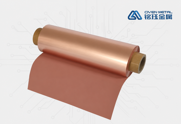
ແຜ່ນທອງແດງຮູບແບບໂປ່ງໃສຕໍ່າຫຼາຍ
ແຜ່ນທອງແດງເຄື່ອນໄຫວທີ່ຖືກເຄື່ອງປະກອບດ້ວຍໄຟຟ້າ ລະດັບຕໍ່າພິເສດ HVLP
ພື້ນຜິວທີ່ລຽບທີ່ສຸດໃນບັນດາແຜ່ນທອງແດງທາງການຄ້າໃນປັດຈຸບັນ, ມີຄ່າ Rz ຕໍ່າເຖິງ 1-1.5 μm. ໄດ້ຖືກອອກແບບມາສຳລັບ mmWave ສູງກວ່າ 28 GHz ແລະ ການເຊື່ອມຕໍ່ຄວາມໄວສູງພິເສດໃນກຸ່ມການຝຶກອົບຮົມ AI, ມັນເປັນວັດສະດຸພື້ນຖານສຳລັບຍຸກການຄິດໄລ່.
· ລັກສະນະຂອງຜະລິດຕະພັນ
- Rz
- Df
- ≥ 56 Gbps
- HVLP-1 ~5 ໄດ້
ແຜນການພັດທະນາຄວາມຂຸ້ນຂ້ຽວຂອງເສັ້ນທາງ
ການວິວັດທະນາການຂອງຄວາມຂຸ່ນຂ້າງຂອງພື້ນຜິວ
ມອບ ຫມາຍ ເຖິງ
ມອບ ຫມາຍ ເຖິງ
HVL ຕັ້ງຄ່າ fuq VLP (ຂ້ອຍແຟ້ມ ແທ້, Rz ≤ 2 μm), ທົດຈໍ່ ເກີດຂໍ້ມູນຂັ້ມ ແຂງ ຂຶ້ນ ເກີດ ຂຶ້ນຊ້ອຍງ ກ່ຽວກັບ Rz ເອົາ 1-1.5 μm ຫຼື ເຖິງ (ຂ້ອຍ HVLP-5 ເກີດຂໍ້ມູນ Rz ≤ 1.0 μm).
Why such an extremely smooth surface? The answer is the skin effect. At high frequencies (especially > 10 GHz), AC current does not flow evenly through the conductor cross-section but concentrates in a very thin "skin depth" layer at the surface; the higher the frequency, the shallower the skin depth. At 28 GHz mmWave, for example, the skin depth of copper is only about 0.4 μm. If the surface peaks and valleys (Rz) of the foil are much larger than the skin depth, current must "crawl" along a tortuous surface, greatly lengthening the effective path, sharply increasing resistance and severely attenuating the signal.
HVLP ກໍາລັງອົບຮົມ ກ່ຽວກັບ ອໍານານ , ຫນ້າ ຫນ້າ ຫນ້າ ຫມາຍ ເຖິງ ຂໍ້ ຫນ້າ ຫນ້າ ຫນ້າ ຫນ້າ ແລະ ຕັດສິນ ໃຈ. ດ້ວຍເຫດນີ້, ການສູນເສຍການສຽບຂອງມັນທີ່ 28 GHz ແລະສູງກວ່າແມ່ນຕໍ່າກວ່າໂຟມ STD ເຖິງ 60-70%. ເກີດຂໍ້ຜິດພາດການ (AII) ຊື້ 56 Gbps / 112 Gbps SerDes rates ແລະ 5G-A / 6G mmWave ໂປຣເເກຣມແກຣມ HVLP ເປັນ ເລື່ອງ ຫນ້າ ທີ່ ບໍ່ສາມາດເປີດ.
ໂປຣເເກຣມແກຣມແກຣມ
- ອວຍລະບົບ: 1.0 - 1.5 μm (HVLP-5 ສາມາດບັນລຸ ≤ 1.0 μm)
- ກ່ຽວກັບແກ້ໄຂຫ້າລະດັບ: HVLP-1 / HVLP-2 / HVLP-3 / HVLP-4 / HVLP-5
- ກ່ຽວກັບ Df: < 0.003 (ລະດับການສູນເສຍຕໍ່າຫຼາຍ)
- ເເລະ ຕັດສິນ ໃຈ @ 10 GHz: ≤ 0.35 dB/in, ຕ່ຳກວ່າ STD ປະມານ 60%
- ປະສົບການສູດ: ≥ 28GHz mmWave/56-112 Gbps ເວລາ ເວລາ SerDes
ການປຽບທຽບຄວາມຂຸ່ນຂົ້ນສູງສຸດຂອງ HVLP
ສະເພາະລັກສະນະ
ໂປຣເເກຣມແກຣມແກຣມແກຣມ
Five sub-grades covering the full high-speed spectrum from 25 Gbps to mmWave.
ຮູບແບບການສະໜອງ
- ມ້ວນ: ກວ້າງສູງສຸດ 1295 mm
- ແຜ່ນ: ສູງສຸດ 1295 × 1295 mm
- HVLP-4/5 ຕາມການສັ່ງຊື້ລ່ວງໜ້າ, ເວລາການຜະລິດ 4-6 ອາທິດ
ວັດສະດຸທີ່ເຂົ້າກັນໄດ້
- PTFE (Ultra Low Los grads)
- ຢາງไฮໂດຣຄາບອນ (Df < 0.003)
- PPE/PPO ປັບປ່ຽນ, LCP ພາດສະຕິກເຄິ່ງແຫຼວ
ຄໍາຮ້ອງສະຫມັກ
ໂປຣເເກຣມແກຣມ
ໃຫ້ບໍລິການແກ່ທຸກພາກສ່ວນສຳຄັນຂອງການຜະລິດເອເລັກໂຕຣນິກ.
ເຊີເວີ AI ແລະ ກຸ່ມຄອມພິວເຕີ
GPU accelerator cards, TPU/NPU training boards, 56–112 Gbps SerDes high-speed interconnects
5G-A / 6G mmWave
28/39/77 GHz mmWave antenna modules, phased array radar transceiver units
Satellite Communications & Radar
Satellite-borne phased arrays, satellite internet ground stations, military electronic warfare systems
Ultra-High-Speed Switches
400GE / 800GE switch backplanes, co-packaged optics (CPO) substrates
Advanced Packaging
Redistribution layers (RDL) in 2.5D/3D IC packaging, conductive layers on glass substrates
Automotive mmWave
77 GHz mmWave radar PCBs, LiDAR control boards
ຂໍ້ດີຫຼັກ
ຂໍ້ດີຂອງຜະລິດຕະພັນຫຼັກ
ສ້າງຂໍ້ໄດ້ປຽບທີ່ແຕກຕ່າງ.
Industry's Lowest Roughness
Rz ≤ 1.5 μm (HVLP-5 reaches ≤ 1.0 μm), approaching the physical limit
Ultra-Low Signal Loss
Df < 0.003, with insertion loss 60%+ lower than STD
Supports 112 Gbps+
Meets the demanding requirements of next-generation AI computing and 6G mmWave
Five-Grade Selection
HVLP-1 to HVLP-5 precisely matched to different frequencies and cost budgets
Compatible with Top Substrates
Validated on ultra-low-loss substrates including PTFE, hydrocarbon resin and LCP
Strategically Scarce Resource
Global capacity is limited, and leading manufacturers have secured long-term supply
Get HVLP Copper Foil Samples & Technical Data
Our technical team can recommend the optimal thickness grade and matching substrate for your specific application.