

ከፍተኛ ፈቃደኛ ሐሳብ
VLP በጣም ታላቅ የኤሌክትሮዴፖዚዝ የተዘጋጀ ኮፐር ፎይል
ለ5G የሐሳብ ግንኙነት ቁልፍ መሠረት ፣ ኤ. በጣም ዝቅተኛ የሆነው አደጋ ስሜት ምልክት ያስተላልፋል ። ግሩም አውራጃ
አልተገኘም >VLP ምንድን ነው?
ቪ ፒፕ በጣም ዝቅተኛ የሆነ ትንቢት ፊደል ምንድን ነው?
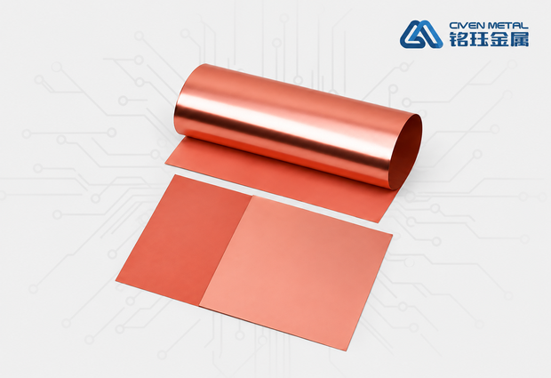
VLP (የጥቂት ምርጫ) ምርጫዎች ወይስ ultra-low profile copper foil, a core category in the low-profile electrodeposited copper foil family. It is produced by precision electrodeposition: a high current density is applied in a copper sulfate plating solution to deposit copper onto a high-speed rotating cathode drum. The finished foil has a smooth drum side and a matte side, both with very low surface roughness (Rz ≤ 2 μm), and its grains are fine and equiaxed rather than conventionally columnar.
Compared with standard electrodeposited foil (STD) and low profile foil (LP), VLP foil has a significantly lower surface profile. This property directly addresses ከፍተኛ ፍጥነት የአውራጃ ወረዳዎች ዋነኛ ፈተና: ከፍተኛ ፈረንሳዎች ቆዳ ውጤት አብዛኛውን ጊዜ ድራማው ገጽ ላይ የሚጓዝበትን ያደርጋል ምልክት ማጣት ይበልጣል በጣም ቆሻሻ ፊት ቪ ፒ ምልክትን ያጠፋል ።
ቁልፍ ሂደት ባሕርይ
- Ultra-low roughness on both sides: both drum side and matte side reach Rz ≤ 2 μm
- ጥሩ ቅንጣት ፦ የተሻለ የኢዮቶሮፕስ ያልተለመደ
- ከፍተኛ ጉልበት ፦ እንደ ፒቲኤኤ እና ሃይድሮካርቦን ስራስን ያሉ ጠንካራ ፍሬዎችን ጠንካር ማሰራጨት
- አነስተኛ ዕቃዎች: ከፍተኛ ንጽሕና ግሩም ድራማነትና መንከባከብ
የፊደል ትንቢት
Surface profile comparison
ምርጫ፦ STD → ላፕ (ጥቂት ፊሊል) → የVLP (መረጠው ምርጫ) → ኤፍ ቪ ፊልም
ፕሮግራሞች
ዋናው ተጠቃሚ እና መጨረሻ ፕሮግራሞችን
VLP ፊል ከፍተኛ አደጋ ለመሥራት ከፍተኛ ፍጥነት ያለው መዳብ ላንዲስት (CCL) የተባለ ጠንካራ የምልክት ንጹሕ አቋማቸውን የሚያስፈልገው በኤሌክትሮኒክስ በስፋት ይጠቀማል፡፡
5G የሐሳብ ግንኙነት መሣሪያ
እንደ መሠረተ ስታታሽ አቴናዎች ፣ RF ፊደል ሞድሶች እና ሚም Wave መሣሪያዎች ያሉ ኮር 5G ሁሉም በጣም አነስተኛ መግቢያ የሚጠይቅ ነው ።
ያይ ሰርከቶች እና የዳታ ማዕከል
ከፍተኛ ሥራ የግሪክኛ ፕሮግራሞች ፣ ኤ. በአንድ ኤይ ሰርቨር ከተለያዩ ስርቨር ፊል እስከ አሥር እጥፍ ሊጠቀም ይችላል፡፡
የኤድ ኤድ ቢቦች
በጣም ስነር ፎንኖች ልብስና ከፍተኛ ፍጻሜ ሙሉ በሙሉ ኤሌክትሮኒክ
ኤሌክትሮኒክስ
EV powertrain control boards, ADAS mmWave radar PCBs, in-vehicle high-speed networks and charging management systems.
የድረ ገጽ የሐሳብ ግንኙነት መሣሪያ
ከፍተኛ ፍጥነት የተለያዩ የጀርባ አውሮፕላኖች ፣ ኦፕቲካል የሐሳብ ሞድሶች ፣ የድረ ግዛቶችና ምርመራና የመለካ መሣሪያዎችን
ሽማግሌዎች የታተሙ ዩኒቨርሲቲ
ቅሬታዎችን ያጠቃሉ ። ቀስ በቀላሉ የሚጠይቁ ሊሆኑ የሚችሉ ሌሎች አማካኝነትና ከፍተኛ ትምክህት የሚጠይቁ ሌሎች አማካኝነትም ።
ምርጫዎች
Available Specifications
በብዙ ውፍረት የተለያዩ ክፍሎች ያላቸውን አማካኝነት ሁሉንም ነገር ከተለመደ ፒፒ B
| Model series | ሙዚቃ | አካባቢ ክብደት | ከፍተኛ ጥፋት | ጥንካሬ | የተለመደ ፕሮግራሞች |
|---|---|---|---|---|---|
| VLP-12E | 12 ሜትር | ~ 107 ግ / m² | ≤ 2.0 μm | ≥ 0.8 kg/cm | HDI multilayer boards, FPC flexible boards |
| VLP-18E | 18 ሜትር | ~ 161 ግ / m² | ≤ 2.0 μm | ≥ 0.9 ኪሎ | High-frequency high-speed multilayer boards, smartphone mainboards |
| VLP-35E | 35 μm | ~ 305 ግ / m² | ≤ 2.0 μm | ≥ 1.0 kg/cm | 5G base stations, AI server mainboards (mainstream grade) |
| VLP-70E | 70 ሜትር | ~ 610 ግ / m² | ≤ 2.5 μm | ≥ 1.0 kg/cm | High-power circuit boards, automotive electronics |
| VLP-105E | 105 ሜሪም | ~915 g/m² | ≤ 2.5 μm | ≥ 1.0 kg/cm | Heavy-copper power boards, defense and aerospace high-frequency boards |
| VLP-HF series | 12–70 μm | Custom | ≤ 1.8 μm | ≥ 1.0 kg/cm | Ultra-high-frequency (≥ 28 GHz) mmWave applications |
ፋይል ምረጡ
- ሮሎኖች ፦ እስከ 1295 ሚም ስፍር
- የገጾች ፦ እስከ 1295 × 1295 ሚልም
Quality Certifications
- IATF 16949 automotive quality management system
- ISO 9001 quality management system certification
- Compliant with IPC-4562 specification for electrodeposited copper foil
Why VLP
Product Advantages
Six core technical advantages, a complete material solution for high-frequency, high-speed PCB manufacturing.
Ultra-Low Signal Transmission Loss
The ultra-smooth Rz ≤ 2 μm surface greatly reduces conductor loss from the skin effect, with Df optimized to ≤ 0.002, ensuring high-speed signal integrity. Ideal for 5G mmWave and high-speed backplanes in AI servers.
Fine-Line Etching Capability
The fine equiaxed grain structure enables faster etching and more uniform side etching, supporting fine lines at L/S = 25/25 μm and below, with significantly fewer white spot defects and higher pattern resolution.
High Bonding Reliability
Achieves peel strength of ≥ 0.8–1.0 kg/cm while maintaining ultra-low roughness, with excellent bonding interfaces on low-loss substrates such as PTFE and hydrocarbon resins and no risk of copper powder transfer.
Precise Characteristic Impedance Control
Uniform thickness and a flat surface minimize signal propagation delay and keep characteristic impedance deviation within ±7%, meeting the strict impedance matching requirements of high-speed differential signals.
Higher Processing Yield
During lamination, the low-profile surface is less likely to pierce thin prepreg (PP) sheets, reducing short-circuit risk. It drills well and suits laser blind via processing, with no copper recrystallization after multiple laminations.
Wide-Temperature Stability
Maintains good mechanical strength and electrical performance at high temperatures (Tg ≥ 180°C), with excellent oxidation and corrosion resistance, extending PCB service life in harsh conditions.
VLP vs Conventional Copper Foil: Key Metrics Compared
| Metric | Standard foil (STD) | VLP very low profile | Improvement |
|---|---|---|---|
| ከፍተኛ ጥፋት | 6–10 μm | ≤ 2 μm | ↓ 70–80% |
| @ 10 ግርድ | > 0.8 dB/in | ≤ 0.4 dB/in | ↓ ~50% |
| Minimum line width / spacing | ≥ 50/50 μm | ≥ 25/25 μm | 2× precision |
| Impedance deviation | ± 10% | ± 7% | ↑ Control precision |
Get VLP Copper Foil Samples & Technical Data
የቴክኖሎጂ ቡድናችን ጥሩ ውድ ውጤትና ውጤታማ የሆነውን ልዩ ልዩ ልዩ ትርጉም ሊያደርግ ይችላሉ ።