

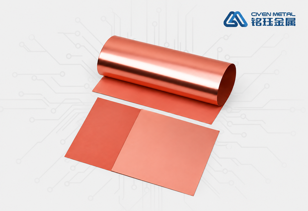
Materyal sa Taas nga Kasak - · Mataas nga Substrat
VLP Mga Kaayo nga Ubos nga Profile nga Gipadagan sa Elektrisidad nga Tumbaga nga Folio
A key base material for 5G communications, AI servers and high-frequency, high-speed PCBs. Its very low surface roughness significantly reduces signal transmission loss and meets the demands of high-density interconnect (HDI) and fine-line manufacturing.
Kontaka Kami >>Unsa ang VLP
Unsa ang VLP nga Very Low Profile Copper Foil?
Ang VLP (Very Low Profile) nagpasabot sa Muyubos nga profile o Ultra-low profile copper foil, a core category in the low-profile electrodeposited copper foil family. It is produced by precision electrodeposition: a high current density is applied in a copper sulfate plating solution to deposit copper onto a high-speed rotating cathode drum. The finished foil has a smooth drum side and a matte side, both with very low surface roughness (Rz ≤ 2 μm), and its grains are fine and equiaxed rather than conventionally columnar.
Kon itandi sa naandang electrodeposited foil (STD) ug low profile foil (LP), ang VLP foil dunay mas ubos nga profile sa ibabaw. Kining maong propiedad direktang naghatag ug adresg Ang pangunang hagit sa taas nga kasukland, kusog nga mga sirkito: at high frequencies, the skin effect causes current to travel mainly along the conductor surface, so the rougher the surface, the greater the signal loss (worsening insertion loss IL and dielectric loss Df). With an extremely flat surface, VLP minimizes signal transmission loss.
Mga Kinaiya sa Pangunang Proseso
- Ultra-low roughness on both sides: Ang duha ka kilid sa tambol ug ang matahum nga bahin makaabot og Rz ≤ 2 μm.
- Maayong mga butang nga may parehas nga gidak-on: dili-kolumnar nga istruktura nga adunay mas maayo nga isotropy
- High peel strength: lig-on nga pagbugkos sa mga substrate nga adunay taas nga frequency sama sa PTFE ug hydrocarbon resins
- Dili kaayo ang alloy: taas nga kaputli uban sa talagsaong conductivity ug resistensya sa pagkadunot
Pagkomparar sa Profile sa Ibabaw
Surface profile comparison
Paglaraw sa teknolohiya: STD → LP (Low Profile) → VLP (Ubdos kaayo nga Profile)→ HVLP (Hyper Very Low Profile)
Mga aplikasyon
Mga Pangunang Gamit ug Katapusan nga Paggamit
Ang VLP foil gikombinar sa mga substrate nga adunay gamay nga pagkawala aron makahimo og taas nga frequency, taas nga katulin nga copper clad laminates (CCL), nga kaylap nga gigamit sa high-end electronics nga adunay higpit nga kinahanglanon sa signal integrity.
5G Communication Equipment
Ang mga punoan nga bahin sa imprastraktura sa 5G sama sa mga antena sa base station, mga modyul sa RF front-end ug mga aparato sa mmWave, tanan nagkinahanglan og kaayo ubos nga pagkawala sa pagsulod.
Mga Server sa AI ug Mga Pusat sa Data
Mga high-performance GPU server, AI accelerator card, high-speed switch ug router. Ang usa ka AI server makagamit og hangtod napulo ka pilo nga VLP/HVLP foil kay sa naandan nga server.
Mga Board sa HDI
Mga multilayer HDI board ug bisan unsang lahi nga fine-line interconnects sa mga smartphone, wearables, ug high-end nga elektronikong konsumidor.
Electronics sa Automotive
EV powertrain control boards, ADAS mmWave radar PCBs, in-vehicle high-speed networks and charging management systems.
Gamit sa Komunikasyon sa Networks
Mga sirkito nga adunay taas nga frequency sa mga backplane sa high-speed switch, optical communication modules, network connectors ug mga instrumento sa pagsulay ug pagsukod.
Mabuklad nga mga Sirkito sa Pag-imprinta (FPC)
Foldable screens, flexible display modules, wearable flexible interconnects and other applications that require thin profiles and high bending reliability.
Mga Detalye
Mabatonang mga Paghubitay
Mga standard ug gipahiangay nga grado sa daghang gibag-on, nga naglangkob sa tanan gikan sa naandan nga PCB hangtod sa labi ka baga nga mga board nga adunay taas nga kusog.
| Model series | Nominal nga gibag-on | Areal nga gibug-aton | Kabag-og sa ibabaw Rz | Kusog sa pagpanghilabot | Mga tipikal nga aplikasyon |
|---|---|---|---|---|---|
| VLP-12E | 12 μm | ~ 107 g / m² | ≤ 2.0 μm | ≥ 0.8 kg/cm | HDI multilayer boards, FPC flexible boards |
| VLP-18E | 18 μm | ~161 g/m² | ≤ 2.0 μm | ≥ 0.9 kg/cm | High-frequency high-speed multilayer boards, smartphone mainboards |
| VLP-35E | 35 μm | ~ 305 g / m² | ≤ 2.0 μm | ≥ 1.0 kg/cm | 5G base stations, AI server mainboards (mainstream grade) |
| VLP-70E | 70 μm | ~610 g/m² | ≤ 2.5 μm | ≥ 1.0 kg/cm | High-power circuit boards, automotive electronics |
| VLP-105E | 105 μm | ~915 g/m² | ≤ 2.5 μm | ≥ 1.0 kg/cm | Heavy-copper power boards, defense and aerospace high-frequency boards |
| VLP-HF series | 12–70 μm | Custom | ≤ 1.8 μm | ≥ 1.0 kg/cm | Ultra-high-frequency (≥ 28 GHz) mmWave applications |
Format sa Suplay
- Mga rolyo: gilapdon hangtod sa 1295 mm
- Mga panid: hangtod sa 1295 × 1295 mm.
Mga Certification sa Kality
- IATF 16949 automotive quality management system
- Sertipikasyon sa sistema sa pagdumala sa kalidad nga ISO 9001
- Compliant with IPC-4562 specification for electrodeposited copper foil
Why VLP
Product Advantages
Six core technical advantages, a complete material solution for high-frequency, high-speed PCB manufacturing.
Ultra-Low Signal Transmission Loss
The ultra-smooth Rz ≤ 2 μm surface greatly reduces conductor loss from the skin effect, with Df optimized to ≤ 0.002, ensuring high-speed signal integrity. Ideal for 5G mmWave and high-speed backplanes in AI servers.
Fine-Line Etching Capability
The fine equiaxed grain structure enables faster etching and more uniform side etching, supporting fine lines at L/S = 25/25 μm and below, with significantly fewer white spot defects and higher pattern resolution.
High Bonding Reliability
Achieves peel strength of ≥ 0.8–1.0 kg/cm while maintaining ultra-low roughness, with excellent bonding interfaces on low-loss substrates such as PTFE and hydrocarbon resins and no risk of copper powder transfer.
Precise Characteristic Impedance Control
Uniform thickness and a flat surface minimize signal propagation delay and keep characteristic impedance deviation within ±7%, meeting the strict impedance matching requirements of high-speed differential signals.
Higher Processing Yield
During lamination, the low-profile surface is less likely to pierce thin prepreg (PP) sheets, reducing short-circuit risk. It drills well and suits laser blind via processing, with no copper recrystallization after multiple laminations.
Wide-Temperature Stability
Maintains good mechanical strength and electrical performance at high temperatures (Tg ≥ 180°C), with excellent oxidation and corrosion resistance, extending PCB service life in harsh conditions.
VLP vs Conventional Copper Foil: Key Metrics Compared
| Metric | Standard foil (STD) | VLP very low profile | Improvement |
|---|---|---|---|
| Kabag-og sa ibabaw Rz | 6–10 μm | ≤ 2 μm | ↓ 70–80% |
| Insertion loss @ 10 GHz | > 0.8 dB/in | ≤ 0.4 dB/in | ↓ ~50% |
| Minimum line width / spacing | ≥ 50/50 μm | ≥ 25/25 μm | 2× precision |
| Impedance deviation | ± 10% | ± 7% | ↑ Control precision |
Get VLP Copper Foil Samples & Technical Data
Ang among teknikal nga tem makarekomendar sa labing maayong pagkabag - on ug sa substrate alang sa imong espesipikong aplikasyon.