

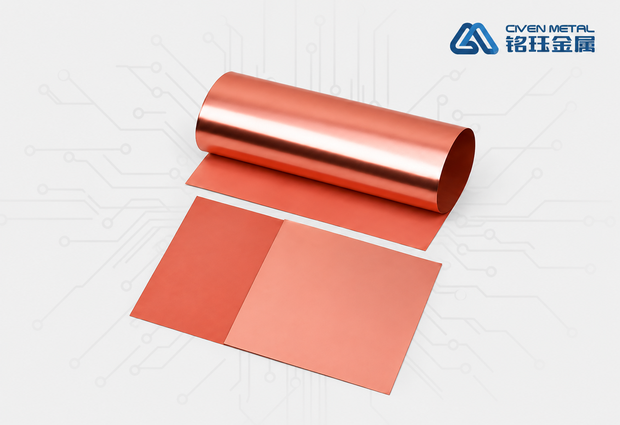
Mataas na Frequency Material · High-Speed Substrate Materiale
VLP Very Low Profile Electrodeposited Copper Foil
Isang pangunahing materyal para sa 5G komunikasyon, AI servers at high-frequency, high-speed PCBs. Ang napakababang magaspang sa ibabaw nito ay nagpapababa ng pagkawala ng signal transmission at nakakatugon sa mga pangangailangan ng high-density interconnect (HDI) at fine-line manufacturing.
Contact Us >>Ano ang VLP
Ano ang VLP Very Low Profile Copper Foil?
Ang VLP (Very Low Profile) ay tumutukoy Mababang profile O Ultra-mababa profile Talper foil, isang pangunahing kategorya sa mababang-profile electrodeposited copper foil family. Ito ay ginawa sa pamamagitan ng tiyak na electrodeposition: isang mataas na kasalukuyang density ay ginagamit sa isang sulfate plating solusyon ng tanso upang deposito ang tanso sa isang mataas na bilis na pag-ikot ng pusa drum. Ang natapos na foil ay may isang makinis na drum bahagi at isang matte bahagi, parehong may napakababang magaspang sa ibabaw (Rz ≤ 2 μm), at ang mga butil nito ay mabuti at equaxed sa halip na konvensyonal na kolonga ..
Kumpara sa standard electrodeposited foil (STD) at mababang profile foil (LP), ang VLP foil ay may malaking mas mababang profile sa ibabaw. Direktang address ng ari-arian Ang pangunahing hamon ng high-frequency, high-speed circuits: Sa mataas na frequency, ang epekto ng balat ay nagdudulot ng kasalukuyang paglalakbay sa ibabaw ng conductor, kaya mas magaspang ang ibabaw, ang mas malaki na pagkawala ng signal (pagpapalabis ng pagkawala ng insertion IL at dielectric loss Df). Sa isang labis na flat na ibabaw, ang VLP ay nagpapahiwatig ng pagkawala ng signal transmission.
Key Process Characteristics
- Ultra-mababang magaspang sa parehong panig: Parehong drum bahagi at matte na bahagi ay umabot sa Rz ≤ 2 μm
- Mabuting butil ng equiaxed: Struktura na hindi columnar na may mas mahusay na isotropy
- Mataas na lakas ng peel: Malakas na bonding sa mga substrates ng high-frequency tulad ng PTFE at hydrocarbon
- Mababang nilalaman ng alloy: Mataas na kalinisan na may mahusay na conductivity at corrosion
Paghahambing sa Surface Profile
Paghahambing sa surface profile
Kalsada sa teknolohiya: STD → LP (Mababang Profile) → VLP (Very Low Profile)→ HVLP (Hyper Very Low Profile)
Mga application
Pangunahing Uses & End Applications
Ang VLP foil ay pinagsama sa mga substrate ng mababang pagkawala upang gumawa ng mataas na frequency, high-speed copper clad laminates (CCL), malawak na ginagamit sa high-end electronics na may mahigpit na pangangailangan sa integrity ng signal.
5G Communication Equipment
Mga bahagi ng core 5G infrastructure tulad ng mga antennas ng base station, modules ng front-end ng RF at mmWave devices, lahat ng nangangailangan ng mababang pagkawala ng insertion.
AI Servers & Data Centers
Mga high-performance GPU servers, AI accelerator cards, high-speed switchs at routers. Ang isang solong AI server ay maaaring gamitin hanggang sampung beses ng maraming VLP/HVLP foil bilang isang konvensyonal na server.
HDI Boards
Multilayer HDI boards at anumang layer fine-line interconects sa smartphones, Mga pagod at mataas na consumer electronics.
Automotive Electronics
EV powertrain control boards, ADAS mmWave radar PCBs, in-hehicle high-speed networks at charging management systems.
Network Communication Equipment
Mga high-frequency circuits sa mga high-speed switch backplanes, mga optical communication module, network connectors at mga instrumento ng pagsusuri at sukat.
Flexible Printed Circuits (FPC)
Mga foldable screen, flexible display modules, Mapagod na flexible interconcts at iba pang mga application na nangangailangan ng manipis na profile at mataas na pagiging maaasahan.
Mga specification
Magagamit na mga Specification
Standard at custom grades sa maraming makapal, na sumasaklaw sa lahat mula sa konvensyonal na PCBs hanggang sa sobrang makapal na mataas na power boards.
| Model series | Nominal na kakalo | Bumagas ng areal | Rughness Rz | Lakas ng Peel | Karaniwang aplikan |
|---|---|---|---|---|---|
| VLP-12E | 12 μm | ~107 g/m² | ≤ 2.0 μm | ≥ 0.8 kg/cm | HDI multilayer boards, FPC flexible boards |
| VLP-18E | 18 μm | ~161 g/m² | ≤ 2.0 μm | ≥ 0.9 kg/cm | High-frequency high-speed multilayer boards, smartphone mainboards |
| VLP-35E | 35 μm | ~305 g/m² | ≤ 2.0 μm | ≥ 1.0 kg/cm | 5G base stations, AI server mainboards (mainstream grade) |
| VLP-70E | 70 μm | ~610 g/m² | ≤ 2.5 μm | ≥ 1.0 kg/cm | High-power circuit boards, automotive electronics |
| VLP-105E | 105 μm | ~915 g/m² | ≤ 2.5 μm | ≥ 1.0 kg/cm | Heavy-copper power boards, defense and aerospace high-frequency boards |
| VLP-HF series | 12–70 μm | Custom | ≤ 1.8 μm | ≥ 1.0 kg/cm | Ultra-high-frequency (≥ 28 GHz) mmWave applications |
Format ng Supply
- Rolls: lawad hanggang 1295 mm.
- Sheets: hanggang 1295 × 1295 mm.
Quality Certifications
- IATF 16949 automotive quality management system
- ISO 9001 quality management system certification
- Compliant with IPC-4562 specification for electrodeposited copper foil
Why VLP
Product Advantages
Six core technical advantages, a complete material solution for high-frequency, high-speed PCB manufacturing.
Ultra-Low Signal Transmission Loss
The ultra-smooth Rz ≤ 2 μm surface greatly reduces conductor loss from the skin effect, with Df optimized to ≤ 0.002, ensuring high-speed signal integrity. Ideal for 5G mmWave and high-speed backplanes in AI servers.
Fine-Line Etching Capability
The fine equiaxed grain structure enables faster etching and more uniform side etching, supporting fine lines at L/S = 25/25 μm and below, with significantly fewer white spot defects and higher pattern resolution.
High Bonding Reliability
Achieves peel strength of ≥ 0.8–1.0 kg/cm while maintaining ultra-low roughness, with excellent bonding interfaces on low-loss substrates such as PTFE and hydrocarbon resins and no risk of copper powder transfer.
Precise Characteristic Impedance Control
Uniform thickness and a flat surface minimize signal propagation delay and keep characteristic impedance deviation within ±7%, meeting the strict impedance matching requirements of high-speed differential signals.
Higher Processing Yield
During lamination, the low-profile surface is less likely to pierce thin prepreg (PP) sheets, reducing short-circuit risk. It drills well and suits laser blind via processing, with no copper recrystallization after multiple laminations.
Wide-Temperature Stability
Maintains good mechanical strength and electrical performance at high temperatures (Tg ≥ 180°C), with excellent oxidation and corrosion resistance, extending PCB service life in harsh conditions.
VLP vs Conventional Copper Foil: Key Metrics Compared
| Metric | Standard foil (STD) | VLP very low profile | Improvement |
|---|---|---|---|
| Rughness Rz | 6–10 μm | ≤ 2 μm | ↓ 70–80% |
| Pagkawala ng Insertion @ 10 GHz | > 0.8 dB/in | ≤ 0.4 dB/in | ↓ ~50% |
| Minimum line width / spacing | ≥ 50/50 μm | ≥ 25/25 μm | 2× precision |
| Impedance deviation | ± 10% | ± 7% | ↑ Control precision |
Get VLP Copper Foil Samples & Technical Data
Maaaring irekomenda ng aming teknikal na koponan ang pinakamainam na grade ng makapal at pagtutugma ng substrate para sa iyong tiyak na aplikasyon.