

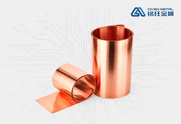
Eine spezielle Kupfer folie, die bei hohen Temperaturen (180 ° C) eine hervorragende Dehnung beibehält: Ihre Hoch temperatur dehnung beträgt mindestens 30% des Raum temperatur werts. Die mehr schicht ige PCB-Laminierung erzeugt eine hohe Wärme, und gewöhnliche Kupfer folie neigt zur Rekristallisation, was zu "Kupfer rissen" in Schaltkreisen der inneren Schicht führt. HTE löst dieses Problem durch eine spezielle Legierung zusammensetzung und Wärme behandlungs prozess. Es ist eine der High-End-Kupfer folien kategorien mit dem größten Marktanteil in China und wird häufig in Mehr schicht platten und High-Tg-Laminaten verwendet.

Elektro abgeschiedene Kupfer folien familie · Vollständige Produkt palette
Hochleistungs-elektro abgeschiedene Kupfer folie: Ein kompletter Bereich von Standard bis Hyper Sehr niedriges Profil
Sechs Serien mit HTE, RTF, LP, VLP, HVLP und BCF mit Dicken von 3,5 bis 420 μm erfüllen alle Anforderungen von herkömmlichen Leiterplatten bis hin zu KI-Servern und 5G mmWave. Jede Klasse ist IPC-4562 zertifiziert und bietet eine zuverlässige Material grundlage für Hochfrequenz-Hoch geschwindigkeit schaltungen.
· Produkt merkmale
- Serie 6, komplette Produktlinie
- Rz ≤ 1 μm niedrigste Rauheit
- 3, 5-420 μm Dicken bereich
- IPC-4562 internat ionale Zertifizierung
Roadmap zur Rauheit entwicklung
Oberflächen rauheit Evolution
Produktreihe
Sechs Kupfer folien serie im Detail
Jede Klasse hat eine klare Rolle: Von kosten sensibler Unterhaltung elektronik bis hin zu anspruchs vollen Hochfrequenz-Hoch geschwindigkeit anwendungen gibt es immer eine, die Ihren Anforderungen entspricht.
Die glänzende Seite der elektro abgelagerten Folie ist ebenfalls aufgeraut, was beiden Seiten eine gute Bindungs festigkeit verleiht. Die beiden Seiten werden unterschied lich stark behandelt: Die dem Dielektrikum zugewandte Seite ist für eine bessere Haftung rauer, während die andere Seite dünner ist, um das Ätzen zu erleichtern. Bei Verwendung als Innen schicht folie in mehr schicht igen Platten entfällt die Schwarz oxid behandlung vor der Laminierung, wodurch die Produktions effizienz verbessert wird. Es ist eine der gängigen Entscheidungen für hoch frequente, kupfer plattierte Hochgeschwindigkeits-Laminate, die Leistung und Kosten ausgleichen.
Ein Übergangs produkt, das zuerst die Oberflächen rauheit auf 3-4 μm brachte. Seine feine Kristalls truktur (< 2 μm) besteht eher aus äquaxen Körnern als aus herkömmlichen säulenförmigen Kristallen mit geschichteter Kristallisation und flachen Graten. Im Vergleich zu STD und RTF ist der Signal übertragungs verlust erheblich geringer, was ihn zu einem kosten günstigen Einstieg in Hoch geschwindigkeit schaltungen macht. Kein Kupfer pulver transfer rückstand nach dem Ätzen und besserer Oberflächen-und Isolation widerstand.
Ultra-smooth copper foil with surface roughness ≤ 2 μm, produced by precision electrodeposition. Both sides reach very low roughness, and the fine equiaxed grain structure ensures isotropy. It greatly reduces conductor loss caused by the skin effect, with Df optimizable to ≤ 0.002, and bonds excellently with low-loss substrates such as PTFE and hydrocarbon resins. It is the mainstay material for high-frequency, high-speed applications such as 5G communications and AI servers.
The smoothest surface among today's commercial copper foils, with Rz as low as 1–1.5 μm or even lower. Building on VLP, it approaches the physical limit of roughness and is designed for mmWave above 28 GHz and ultra-high-speed interconnects in AI training clusters. A single high-end AI server can use up to ten times as much HVLP as a conventional server. As global computing infrastructure expands, supply remains tight.
Electrodeposited copper foil dedicated to lithium-ion battery anode current collectors and one of the core base materials of lithium batteries. Unlike PCB copper foil, BCF has a double-shiny (bright on both sides) surface finish and is soft enough for battery winding processes, while offering excellent chemical and electrochemical stability. Thinner foil is the key path to higher energy density: reducing thickness from 12 μm to 6 μm or even 4–5 μm directly cuts battery weight by about 5–9% and lowers internal resistance, improving charge-discharge efficiency.
Selection Guide
How to Choose the Right Copper Foil
Quickly identify the best solution based on signal rate, loss budget and application.
📐 Supply Format
- Rollen: Breite bis zu 1295 mm
- Blätter: bis zu 1295 × 1295 mm
- Custom thicknesses and special widths available
✓ Quality Certifications
- IATF 16949 automotive quality management system
- ISO 9001 quality management system certification
- Compliant with IPC-4562 international specification for electrodeposited copper foil
- Compliant with GB/T 5230-2020 national standard
Anwendungen
End-Use Applications Overview
From consumer electronics to cutting-edge computing infrastructure, our full range of copper foils covers every key sector of electronics manufacturing.
5G Communications Infrastructure
Base station antennas, RF front ends, mmWave modules. VLP/HVLP paired with PTFE substrates minimizes insertion loss.
KI-Server & Rechen zentren
GPU accelerator cards, high-performance mainboards, high-speed switch backplanes. HVLP-4/5 is a core enabling material for today's AI computing hardware.
HDI-Verbindung mit hoher Dichte
Any-layer interconnect boards for smartphones, tablets and wearables. UTF + RCC enables fine lines down to L/S ≤ 20/20 μm.
Automobile lektronik
EV power control, ADAS mmWave radar, in-vehicle networking and charging management. HTE/VLP meets automotive-grade reliability requirements.
Netzwerk kommunikation ausrüstung
High-speed switches, routers, optical communication modules, test and measurement instruments. RTF/VLP is the mainstream choice for mid- to high-speed digital circuits.
Flexible Circuits (FPC)
Foldable screens, flexible display modules, wearable interconnects. Ultra-thin VLP/HVLP grades on PI substrates enable extremely thin, bendable designs.
IC Packaging & Substrates
Semiconductor package substrates, substrate-like PCBs (SLP), FC-BGA substrates. Ultra-thin 5–9 μm UTF supports fine routing for advanced packaging.
Defense & Aerospace
High-power high-frequency boards, phased array radar, satellite communication terminals. Extra-thick VLP-HTE grades (3–12 oz) withstand extreme operating conditions.
Kern vorteile
Why Choose Our Copper Foil
Differentiated competitiveness across six dimensions.
Complete Roughness Range
From 7–8 μm for STD to ≤ 1.5 μm for HVLP, nine series form a seamless product matrix, with an optimal choice for any signal rate.
Industry-Leading High-Frequency Loss
VLP/HVLP Df values go below 0.002, with insertion loss more than 50% lower than STD; measured data benchmarks against top international brands.
Wide Thickness Coverage
From ultra-thin 3.5 μm to extra-thick 420 μm, with roll widths up to 1295 mm, one supplier can meet all your sourcing needs from HDI to high-power boards and from PCBs to lithium batteries.
Breite Substrat kompatibilität
PTFE, hydrocarbon resins, modified epoxy, BT resin, CE build-up laminates: all our copper foils are bond-strength verified on mainstream substrate systems.
Stable High-Volume Delivery
IATF 16949 + ISO 9001 dual-certified lines with ample monthly capacity, supplying leading CCL manufacturers and PCB companies in volume for many years.
Customized Technical Service
Our technical support team can recommend the optimal copper foil grade based on your laminate formulation, layer stack-up and target frequency, and help complete reliability validation.
Get Samples & Technical Data
Free samples are available for the full range, and our technical team will provide one-on-one selection advice.