

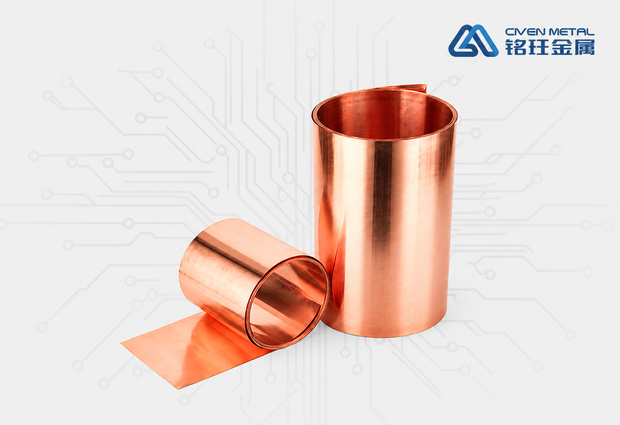
Una lamina di rame speciale che mantiene un eccellente allungamento ad alta temperatura (180 ° C): il suo allungamento ad alta temperatura è almeno il 30% del valore della temperatura ambiente. La laminazione di PCB multistrato genera calore elevato e la normale lamina di rame tende a ricristallizzarsi, causando "crepe di rame" nei circuiti dello strato interno. HTE risolve questo problema attraverso una speciale composizione della lega e un processo di trattamento termico. È una delle categorie di lamina di rame di fascia alta con la più grande quota di mercato in Cina ed è ampiamente utilizzata nelle tavole multistrato e nei laminati high-Tg.

Famiglia di lamina di rame elettrodepositata · Gamma completa di prodotti
Stagnola di rame elettrodepositata ad alte prestazioni: una gamma completa da standard a profilo iper molto basso
Sei serie che coprono HTE, RTF, LP, VLP, HVLP e BCF, con spessori da 3,5 a 420 μm, soddisfacendo ogni esigenza, dai PCB convenzionali ai server AI e mmWave 5G. Ogni grado è IPC-4562 certificato, fornendo una base materiale affidabile per circuiti ad alta frequenza e ad alta velocità.
· Caratteristiche del prodotto
- Serie 6, linea di prodotti completa
- Rz ≤ 1 μm rugosità più bassa
- Intervallo di spessore 3, 5-420 μm
- IPC-4562 certificazione internazionale
Roadmap di evoluzione rugosità
Evoluzione della rugosità superficiale
Serie del prodotto
Sei serie di lamina di rame in dettaglio
Ogni grado ha un ruolo chiaro: dall'elettronica di consumo sensibile ai costi alle applicazioni esigenti ad alta frequenza e ad alta velocità, ce n' è sempre una che si adatta alle tue esigenze.
Anche il lato lucido della lamina elettrodepositata è ruvido, conferendo a entrambi i lati una buona forza di legame. I due lati sono trattati in gradi diversi: il lato rivolto verso il dielettrico è più ruvido per una migliore adesione, mentre l'altro lato è più sottile per una più facile incisione. Quando viene utilizzato come foglio di strato interno in tavole multistrato, elimina il trattamento di ossido nero prima della laminazione, migliorando l'efficienza produttiva. È una delle scelte principali per laminati rivestiti in rame ad alta frequenza e alta velocità, bilanciando prestazioni e costi.
Un prodotto di transizione che per primo ha portato la rugosità della superficie al livello di 3-4 μm. La sua struttura cristallina fine (< 2 μm) è costituita da grani equiassati piuttosto che da cristalli colonnari convenzionali, con cristallizzazione stratificata e creste piatte. Rispetto a STD e RTF, la perdita di trasmissione del segnale è significativamente inferiore, rendendola un ingresso conveniente nei circuiti ad alta velocità. Nessun residuo di trasferimento di polvere di rame dopo l'incisione e una migliore resistenza alla superficie e all'isolamento.
Ultra-smooth copper foil with surface roughness ≤ 2 μm, produced by precision electrodeposition. Both sides reach very low roughness, and the fine equiaxed grain structure ensures isotropy. It greatly reduces conductor loss caused by the skin effect, with Df optimizable to ≤ 0.002, and bonds excellently with low-loss substrates such as PTFE and hydrocarbon resins. It is the mainstay material for high-frequency, high-speed applications such as 5G communications and AI servers.
The smoothest surface among today's commercial copper foils, with Rz as low as 1–1.5 μm or even lower. Building on VLP, it approaches the physical limit of roughness and is designed for mmWave above 28 GHz and ultra-high-speed interconnects in AI training clusters. A single high-end AI server can use up to ten times as much HVLP as a conventional server. As global computing infrastructure expands, supply remains tight.
Electrodeposited copper foil dedicated to lithium-ion battery anode current collectors and one of the core base materials of lithium batteries. Unlike PCB copper foil, BCF has a double-shiny (bright on both sides) surface finish and is soft enough for battery winding processes, while offering excellent chemical and electrochemical stability. Thinner foil is the key path to higher energy density: reducing thickness from 12 μm to 6 μm or even 4–5 μm directly cuts battery weight by about 5–9% and lowers internal resistance, improving charge-discharge efficiency.
Selection Guide
How to Choose the Right Copper Foil
Quickly identify the best solution based on signal rate, loss budget and application.
📐 Supply Format
- Rotoli: larghezza fino a 1295 mm
- Fogli: fino a 1295 × 1295 mm
- Custom thicknesses and special widths available
✓ Quality Certifications
- IATF 16949 automotive quality management system
- Certificazione del sistema di gestione della qualità ISO 9001
- Compliant with IPC-4562 international specification for electrodeposited copper foil
- Compliant with GB/T 5230-2020 national standard
Applicazioni
End-Use Applications Overview
From consumer electronics to cutting-edge computing infrastructure, our full range of copper foils covers every key sector of electronics manufacturing.
5G Communications Infrastructure
Base station antennas, RF front ends, mmWave modules. VLP/HVLP paired with PTFE substrates minimizes insertion loss.
Server e centri dati AI
GPU accelerator cards, high-performance mainboards, high-speed switch backplanes. HVLP-4/5 is a core enabling material for today's AI computing hardware.
Interconnessione ad alta densità HDI
Any-layer interconnect boards for smartphones, tablets and wearables. UTF + RCC enables fine lines down to L/S ≤ 20/20 μm.
Elettronica automobilistica
EV power control, ADAS mmWave radar, in-vehicle networking and charging management. HTE/VLP meets automotive-grade reliability requirements.
Apparecchiature di comunicazione di rete
High-speed switches, routers, optical communication modules, test and measurement instruments. RTF/VLP is the mainstream choice for mid- to high-speed digital circuits.
Flexible Circuits (FPC)
Foldable screens, flexible display modules, wearable interconnects. Ultra-thin VLP/HVLP grades on PI substrates enable extremely thin, bendable designs.
IC Packaging & Substrates
Semiconductor package substrates, substrate-like PCBs (SLP), FC-BGA substrates. Ultra-thin 5–9 μm UTF supports fine routing for advanced packaging.
Defense & Aerospace
High-power high-frequency boards, phased array radar, satellite communication terminals. Extra-thick VLP-HTE grades (3–12 oz) withstand extreme operating conditions.
Vantaggi principali
Why Choose Our Copper Foil
Differentiated competitiveness across six dimensions.
Complete Roughness Range
From 7–8 μm for STD to ≤ 1.5 μm for HVLP, nine series form a seamless product matrix, with an optimal choice for any signal rate.
Industry-Leading High-Frequency Loss
VLP/HVLP Df values go below 0.002, with insertion loss more than 50% lower than STD; measured data benchmarks against top international brands.
Wide Thickness Coverage
From ultra-thin 3.5 μm to extra-thick 420 μm, with roll widths up to 1295 mm, one supplier can meet all your sourcing needs from HDI to high-power boards and from PCBs to lithium batteries.
Ampia compatibilità del substrato
PTFE, hydrocarbon resins, modified epoxy, BT resin, CE build-up laminates: all our copper foils are bond-strength verified on mainstream substrate systems.
Stable High-Volume Delivery
IATF 16949 + ISO 9001 dual-certified lines with ample monthly capacity, supplying leading CCL manufacturers and PCB companies in volume for many years.
Customized Technical Service
Our technical support team can recommend the optimal copper foil grade based on your laminate formulation, layer stack-up and target frequency, and help complete reliability validation.
Get Samples & Technical Data
Free samples are available for the full range, and our technical team will provide one-on-one selection advice.