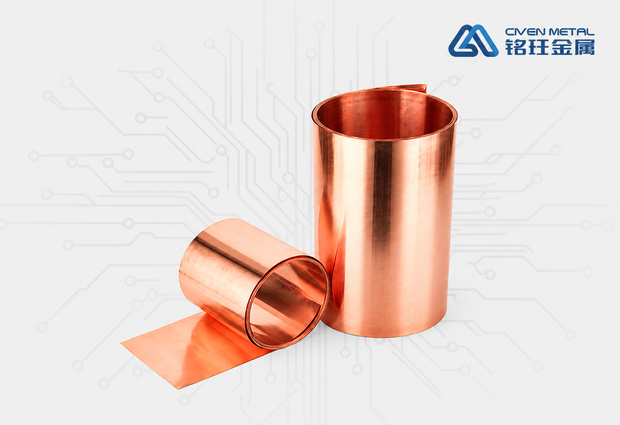
고온 (180 ° C) 에서 우수한 신장을 유지하는 특수 구리 호일: 고온 신장은 실내 온도 값의 30% 이상입니다. 다층 PCB 라미네이션은 높은 열을 발생시키고 일반 구리 포일은 재결정화되어 내부 층 회로에 "구리 균열" 을 일으키는 경향이 있습니다. HTE는 특수 합금 조성 및 열처리 공정을 통해이 문제를 해결합니다. 그것은 중국에서 가장 큰 시장 점유율을 가진 하이 엔드 구리 호일 카테고리 중 하나이며 다층 보드 및 높은 Tg 라미네이트에 널리 사용됩니다.

전기 증착 구리 호일 패밀리 · 전체 제품 범위
고성능 전기 증착 구리 호일: 표준에서 하이퍼까지의 완벽한 범위 매우 낮은 프로필
3.5 ~ 420 μm 두께의 HTE, RTF, LP, VLP, HVLP 및 BCF를 포함하는 6 개의 시리즈는 기존 PCB에서 AI 서버 및 5G mmWave에 이르기까지 모든 요구를 충족시킵니다. 모든 등급은 IPC-4562 인증을 받아 고주파·고속 회로를 위한 신뢰할 수 있는 재료 기반을 제공합니다.
· 제품 특징
- 6 시리즈, 완전한 제품 라인
- Rz ≤ 1 μm 최저 거칠기
- 3.5-420 μm 두께 범위
- IPC-4562 국제 인증
거칠기 진화 로드맵
표면 거칠기 진화
제품 시리즈
세부 사항에 6 개의 구리 호일 시리즈
각 등급에는 명확한 역할이 있습니다. 비용에 민감한 가전 제품에서 까다로운 고주파 고속 응용 프로그램에 이르기까지 항상 귀하의 요구에 맞는 것이 있습니다.
전착 된 호일의 반짝이는 측면도 거칠어져서 양면에 좋은 결합 강도를 제공합니다. 두 측면은 서로 다른 정도로 처리됩니다. 유전체를 향한 측면은 더 나은 접착력을 위해 더 거칠고 다른 측면은 더 쉽게 에칭하기 위해 더 얇습니다. 다층 보드에서 내부 층 호일로 사용될 때, 적층 전에 흑산화물 처리를 제거하여 생산 효율을 향상시킵니다. 그것은 고성능, 고속 구리 클래드 라미네이트의 주류 선택 중 하나이며 성능과 비용의 균형을 유지합니다.
표면 거칠기를 처음으로 3~4μm 수준까지 낮춘 전환형 제품입니다. 미세 결정 구조 (< 2 μm) 는 기존의 원주 결정이 아닌 등축 입자로 구성되며, 층상 결정화와 평평한 융기가 있습니다. STD 및 RTF에 비해 신호 전송 손실이 현저히 낮아 고속 회로로의 비용 효율적인 진입이 가능합니다. 에칭 후 구리 분말 전송 잔류 물이 없으며 표면 및 절연 저항이 우수합니다.
Ultra-smooth copper foil with surface roughness ≤ 2 μm, produced by precision electrodeposition. Both sides reach very low roughness, and the fine equiaxed grain structure ensures isotropy. It greatly reduces conductor loss caused by the skin effect, with Df optimizable to ≤ 0.002, and bonds excellently with low-loss substrates such as PTFE and hydrocarbon resins. It is the mainstay material for high-frequency, high-speed applications such as 5G communications and AI servers.
The smoothest surface among today's commercial copper foils, with Rz as low as 1–1.5 μm or even lower. Building on VLP, it approaches the physical limit of roughness and is designed for mmWave above 28 GHz and ultra-high-speed interconnects in AI training clusters. A single high-end AI server can use up to ten times as much HVLP as a conventional server. As global computing infrastructure expands, supply remains tight.
Electrodeposited copper foil dedicated to lithium-ion battery anode current collectors and one of the core base materials of lithium batteries. Unlike PCB copper foil, BCF has a double-shiny (bright on both sides) surface finish and is soft enough for battery winding processes, while offering excellent chemical and electrochemical stability. Thinner foil is the key path to higher energy density: reducing thickness from 12 μm to 6 μm or even 4–5 μm directly cuts battery weight by about 5–9% and lowers internal resistance, improving charge-discharge efficiency.
Selection Guide
How to Choose the Right Copper Foil
Quickly identify the best solution based on signal rate, loss budget and application.
📐 Supply Format
- 롤: 폭 1295 mm
- 시트: 최대 1295 × 1295 mm
- Custom thicknesses and special widths available
✓ Quality Certifications
- IATF 16949 automotive quality management system
- ISO 9001 quality management system certification
- Compliant with IPC-4562 international specification for electrodeposited copper foil
- Compliant with GB/T 5230-2020 national standard
응용 프로그램
End-Use Applications Overview
From consumer electronics to cutting-edge computing infrastructure, our full range of copper foils covers every key sector of electronics manufacturing.
5G Communications Infrastructure
Base station antennas, RF front ends, mmWave modules. VLP/HVLP paired with PTFE substrates minimizes insertion loss.
AI 서버 및 데이터 센터
GPU accelerator cards, high-performance mainboards, high-speed switch backplanes. HVLP-4/5 is a core enabling material for today's AI computing hardware.
HDI 고밀도 상호 연결
Any-layer interconnect boards for smartphones, tablets and wearables. UTF + RCC enables fine lines down to L/S ≤ 20/20 μm.
자동차 전자
EV power control, ADAS mmWave radar, in-vehicle networking and charging management. HTE/VLP meets automotive-grade reliability requirements.
네트워크 통신 장비
High-speed switches, routers, optical communication modules, test and measurement instruments. RTF/VLP is the mainstream choice for mid- to high-speed digital circuits.
Flexible Circuits (FPC)
Foldable screens, flexible display modules, wearable interconnects. Ultra-thin VLP/HVLP grades on PI substrates enable extremely thin, bendable designs.
IC Packaging & Substrates
Semiconductor package substrates, substrate-like PCBs (SLP), FC-BGA substrates. Ultra-thin 5–9 μm UTF supports fine routing for advanced packaging.
Defense & Aerospace
High-power high-frequency boards, phased array radar, satellite communication terminals. Extra-thick VLP-HTE grades (3–12 oz) withstand extreme operating conditions.
Core Advantages
Why Choose Our Copper Foil
Differentiated competitiveness across six dimensions.
Complete Roughness Range
From 7–8 μm for STD to ≤ 1.5 μm for HVLP, nine series form a seamless product matrix, with an optimal choice for any signal rate.
Industry-Leading High-Frequency Loss
VLP/HVLP Df values go below 0.002, with insertion loss more than 50% lower than STD; measured data benchmarks against top international brands.
Wide Thickness Coverage
From ultra-thin 3.5 μm to extra-thick 420 μm, with roll widths up to 1295 mm, one supplier can meet all your sourcing needs from HDI to high-power boards and from PCBs to lithium batteries.
Broad Substrate Compatibility
PTFE, hydrocarbon resins, modified epoxy, BT resin, CE build-up laminates: all our copper foils are bond-strength verified on mainstream substrate systems.
Stable High-Volume Delivery
IATF 16949 + ISO 9001 dual-certified lines with ample monthly capacity, supplying leading CCL manufacturers and PCB companies in volume for many years.
Customized Technical Service
Our technical support team can recommend the optimal copper foil grade based on your laminate formulation, layer stack-up and target frequency, and help complete reliability validation.
Get Samples & Technical Data
Free samples are available for the full range, and our technical team will provide one-on-one selection advice.